

How To Get Usb Registers Of Chipset
A system on a chip (SoC; es-oh-SEE or sock [nb i]), also written equally system-on-a-chip and system-on-flake, is an integrated circuit (also known as a "chip") that integrates all or near components of a computer or other electronic organization. These components most e'er include a central processing unit (CPU), memory interfaces, on-fleck input/output devices and secondary storage interfaces, ofttimes aslope other components such as radio modems and a graphics processing unit (GPU) – all on a single substrate or microchip.[i] It may contain digital, analog, mixed-betoken, and often radio frequency bespeak processing functions (otherwise it is considered only an application processor).
Higher-performance SoCs are ofttimes paired with defended and physically separate retentivity and secondary storage (such as LPDDR and eUFS or eMMC, respectively) fries, that may be layered on top of the SoC in what'due south known as a parcel on package (Pop) configuration, or be placed close to the SoC. Additionally, SoCs may use separate wireless modems.[two]
SoCs are in contrast to the common traditional motherboard-based PC architecture, which separates components based on role and connects them through a central interfacing circuit lath.[nb 2] Whereas a motherboard houses and connects detachable or replaceable components, SoCs integrate all of these components into a single integrated circuit. An SoC will typically integrate a CPU, graphics and retentivity interfaces,[nb 3] hard-disk and USB connectivity,[nb 4] random-admission and read-merely memories and secondary storage and/or their controllers on a single circuit die, whereas a motherboard would connect these modules equally discrete components or expansion cards.
An SoC integrates a microcontroller, microprocessor or perhaps several processor cores with peripherals like a GPU, Wi-Fi and cellular network radio modems, and/or ane or more coprocessors. Similar to how a microcontroller integrates a microprocessor with peripheral circuits and memory, an SoC tin exist seen as integrating a microcontroller with fifty-fifty more advanced peripherals.
More tightly integrated calculator system designs improve performance and reduce power consumption equally well as semiconductor dice area than multi-chip designs with equivalent functionality. This comes at the cost of reduced replaceability of components. By definition, SoC designs are fully or nearly fully integrated across different component modules. For these reasons, there has been a full general trend towards tighter integration of components in the computer hardware industry, in part due to the influence of SoCs and lessons learned from the mobile and embedded computing markets. SoCs can be viewed every bit function of a larger trend towards embedded computing and hardware acceleration.
SoCs are very common in the mobile calculating (such as in smartphones and tablet computers) and edge computing markets.[3] [four] They are also unremarkably used in embedded systems such as WiFi routers and the Internet of things.
Types [edit]
In full general, there are three distinguishable types of SoCs:
- SoCs congenital effectually a microcontroller,
- SoCs built around a microprocessor, often constitute in mobile phones;
- Specialized application-specific integrated circuit SoCs designed for specific applications that do not fit into the to a higher place two categories
Applications [edit]
SoCs can be practical to whatsoever computing job. Notwithstanding, they are typically used in mobile computing such as tablets, smartphones, smartwatches and netbooks too as embedded systems and in applications where previously microcontrollers would exist used.
Embedded systems [edit]
Where previously only microcontrollers could be used, SoCs are rising to prominence in the embedded systems market. Tighter system integration offers meliorate reliability and mean time betwixt failure, and SoCs offer more than advanced functionality and computing ability than microcontrollers.[5] Applications include AI dispatch, embedded machine vision,[half-dozen] data collection, telemetry, vector processing and ambient intelligence. Often embedded SoCs target the cyberspace of things, industrial net of things and border calculating markets.
Mobile calculating [edit]
Mobile computing based SoCs ever bundle processors, memories, on-chip caches, wireless networking capabilities and often digital camera hardware and firmware. With increasing memory sizes, high finish SoCs volition often take no retentivity and flash storage and instead, the memory and flash retention will exist placed right next to, or above (package on package), the SoC.[seven] Some examples of mobile calculating SoCs include:
- Samsung Electronics: list, typically based on ARM
- Exynos, used mainly by Samsung'southward Galaxy serial of smartphones
- Qualcomm:
- Snapdragon (list), used in many LG, Xiaomi, Google Pixel, HTC and Samsung Galaxy smartphones. In 2018, Snapdragon SoCs are being used every bit the courage of laptop computers running Windows 10, marketed as "Ever Connected PCs".[viii] [9]
Personal computers [edit]
In 1992, Acorn Computers produced the A3010, A3020 and A4000 range of personal computers with the ARM250 SoC. It combined the original Acorn ARM2 processor with a memory controller (MEMC), video controller (VIDC), and I/O controller (IOC). In previous Acorn ARM-powered computers, these were iv detached chips. The ARM7500 chip was their second-generation SoC, based on the ARM700, VIDC20 and IOMD controllers, and was widely licensed in embedded devices such equally gear up-top-boxes, as well as later Acorn personal computers.
SoCs are being applied to mainstream personal computers as of 2018.[8] They are particularly applied to laptops and tablet PCs. Tablet and laptop manufacturers accept learned lessons from embedded systems and smartphone markets virtually reduced ability consumption, ameliorate functioning and reliability from tighter integration of hardware and firmware modules, and LTE and other wireless network communications integrated on chip (integrated network interface controllers).[10]
ARM-based:
- Qualcomm Snapdragon[9]
- ARM250
- ARM7500(FE)
- Apple M1
x86-based:
- Intel Core CULV
Structure [edit]
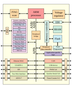
An SoC consists of hardware functional units, including microprocessors that run software code, besides as a communications subsystem to connect, control, direct and interface between these functional modules.
Functional components [edit]
Processor cores [edit]
An SoC must have at to the lowest degree one processor core, but typically an SoC has more than one core. Processor cores tin be a microcontroller, microprocessor (μP),[11] digital signal processor (DSP) or application-specific instruction ready processor (ASIP) core.[12] ASIPs have educational activity sets that are customized for an awarding domain and designed to be more efficient than full general-purpose instructions for a specific type of workload. Multiprocessor SoCs accept more than one processor cadre by definition.
Whether unmarried-cadre, multi-core or manycore, SoC processor cores typically use RISC instruction set architectures. RISC architectures are advantageous over CISC processors for SoCs because they require less digital logic, and therefore less power and surface area on board, and in the embedded and mobile calculating markets, area and power are ofttimes highly constrained. In particular, SoC processor cores often utilise the ARM architecture because it is a soft processor specified every bit an IP cadre and is more power efficient than x86.[11]
Memory [edit]
SoCs must accept semiconductor retentiveness blocks to perform their ciphering, as do microcontrollers and other embedded systems. Depending on the application, SoC memory may form a retentiveness hierarchy and enshroud bureaucracy. In the mobile calculating market place, this is common, but in many low-power embedded microcontrollers, this is non necessary. Memory technologies for SoCs include read-merely memory (ROM), random-access memory (RAM), Electrically Erasable Programmable ROM (EEPROM) and flash memory.[eleven] As in other computer systems, RAM tin can be subdivided into relatively faster but more expensive static RAM (SRAM) and the slower but cheaper dynamic RAM (DRAM). When an SoC has a cache hierarchy, SRAM volition usually be used to implement processor registers and cores' L1 caches whereas DRAM volition be used for lower levels of the cache hierarchy including master memory. "Master retentiveness" may be specific to a single processor (which can be multi-core) when the SoC has multiple processors, in which case it is distributed retentiveness and must be sent via § Intermodule communication on-chip to be accessed by a different processor.[12] For further give-and-take of multi-processing retentiveness issues, run across cache coherence and memory latency.
Interfaces [edit]
SoCs include external interfaces, typically for communication protocols. These are often based upon industry standards such as USB, FireWire, Ethernet, USART, SPI, HDMI, I²C, etc. These interfaces will differ according to the intended application. Wireless networking protocols such every bit Wi-Fi, Bluetooth, 6LoWPAN and virtually-field communication may also exist supported.
When needed, SoCs include analog interfaces including analog-to-digital and digital-to-analog converters, often for signal processing. These may be able to interface with unlike types of sensors or actuators, including smart transducers. They may interface with application-specific modules or shields.[nb five] Or they may be internal to the SoC, such equally if an analog sensor is congenital in to the SoC and its readings must be converted to digital signals for mathematical processing.
Digital bespeak processors [edit]
Digital bespeak processor (DSP) cores are ofttimes included on SoCs. They perform point processing operations in SoCs for sensors, actuators, information drove, data assay and multimedia processing. DSP cores typically feature very long instruction give-and-take (VLIW) and single didactics, multiple data (SIMD) teaching set architectures, and are therefore highly amenable to exploiting didactics-level parallelism through parallel processing and superscalar execution.[12] : iv DSP cores most oft feature application-specific instructions, and as such are typically application-specific instruction-fix processors (ASIP). Such application-specific instructions represent to dedicated hardware functional units that compute those instructions.
Typical DSP instructions include multiply-accumulate, Fast Fourier transform, fused multiply-add together, and convolutions.
Other [edit]
As with other computer systems, SoCs require timing sources to generate clock signals, control execution of SoC functions and provide time context to signal processing applications of the SoC, if needed. Popular fourth dimension sources are crystal oscillators and stage-locked loops.
SoC peripherals including counter-timers, real-time timers and power-on reset generators. SoCs also include voltage regulators and power management circuits.
Intermodule communication [edit]
SoCs comprise many execution units. These units must frequently send data and instructions dorsum and forth. Considering of this, all simply the most footling SoCs require communications subsystems. Originally, every bit with other microcomputer technologies, data charabanc architectures were used, just recently designs based on thin intercommunication networks known as networks-on-chip (NoC) accept risen to prominence and are forecast to overtake bus architectures for SoC design in the near future.[13]
Bus-based advice [edit]
Historically, a shared global estimator bus typically continued the different components, also called "blocks" of the SoC.[13] A very mutual bus for SoC communications is ARM's royalty-gratuitous Advanced Microcontroller Charabanc Architecture (AMBA) standard.
Direct retention access controllers route data straight betwixt external interfaces and SoC memory, bypassing the CPU or command unit, thereby increasing the data throughput of the SoC. This is similar to some device drivers of peripherals on component-based multi-chip module PC architectures.
Computer buses are limited in scalability, supporting but up to tens of cores (multicore) on a single scrap.[13] : xiii Wire filibuster is not scalable due to continued miniaturization, system operation does non scale with the number of cores fastened, the SoC'due south operating frequency must decrease with each additional cadre attached for ability to exist sustainable, and long wires consume big amounts of electric power. These challenges are prohibitive to supporting manycore systems on fleck.[13] : xiii
Network on a chip [edit]
In the late 2010s, a trend of SoCs implementing communications subsystems in terms of a network-like topology instead of bus-based protocols has emerged. A trend towards more processor cores on SoCs has caused on-flake communication efficiency to become one of the key factors in determining the overall organization functioning and cost.[13] : xiii This has led to the emergence of interconnection networks with router-based packet switching known as "networks on scrap" (NoCs) to overcome the bottlenecks of jitney-based networks.[13] : xiii
Networks-on-chip have advantages including destination- and application-specific routing, greater power efficiency and reduced possibility of bus contention. Network-on-bit architectures take inspiration from communication protocols similar TCP and the Cyberspace protocol suite for on-chip communication,[13] although they typically have fewer network layers. Optimal network-on-chip network architectures are an ongoing area of much research interest. NoC architectures range from traditional distributed computing network topologies such equally torus, hypercube, meshes and tree networks to genetic algorithm scheduling to randomized algorithms such as random walks with branching and randomized time to live (TTL).
Many SoC researchers consider NoC architectures to be the future of SoC design because they accept been shown to efficiently meet power and throughput needs of SoC designs. Current NoC architectures are ii-dimensional. 2D IC blueprint has express floorplanning choices as the number of cores in SoCs increment, and so as three-dimensional integrated circuits (3DICs) emerge, SoC designers are looking towards edifice three-dimensional on-chip networks known as 3DNoCs.[13]
Design flow [edit]

A system on a chip consists of both the hardware, described in § Structure, and the software controlling the microcontroller, microprocessor or digital betoken processor cores, peripherals and interfaces. The design flow for an SoC aims to develop this hardware and software at the same fourth dimension, also known as architectural co-design. The design catamenia must also take into account optimizations (§ Optimization goals) and constraints.
Most SoCs are adult from pre-qualified hardware component IP core specifications for the hardware elements and execution units, collectively "blocks", described above, together with software device drivers that may control their functioning. Of particular importance are the protocol stacks that drive industry-standard interfaces like USB. The hardware blocks are put together using computer-aided design tools, specifically electronic design automation tools; the software modules are integrated using a software integrated development environment.
SoCs components are also often designed in high-level programming languages such equally C++, MATLAB or SystemC and converted to RTL designs through loftier-level synthesis (HLS) tools such every bit C to HDL or flow to HDL.[fourteen] HLS products called "algorithmic synthesis" permit designers to use C++ to model and synthesize system, circuit, software and verification levels all in one high level language ordinarily known to computer engineers in a fashion independent of fourth dimension scales, which are typically specified in HDL.[15] Other components can remain software and be compiled and embedded onto soft-core processors included in the SoC every bit modules in HDL as IP cores.
Once the architecture of the SoC has been defined, whatsoever new hardware elements are written in an abstruse hardware description language termed register transfer level (RTL) which defines the circuit behavior, or synthesized into RTL from a high level linguistic communication through high-level synthesis. These elements are connected together in a hardware description linguistic communication to create the full SoC design. The logic specified to connect these components and catechumen betwixt possibly unlike interfaces provided by dissimilar vendors is called mucilage logic.
Design verification [edit]
Chips are verified for validation definiteness earlier being sent to a semiconductor foundry. This process is called functional verification and information technology accounts for a meaning portion of the time and energy expended in the bit design life cycle, often quoted as 70%.[16] [17] With the growing complexity of chips, hardware verification languages like SystemVerilog, SystemC, e, and OpenVera are being used. Bugs found in the verification stage are reported to the designer.
Traditionally, engineers have employed simulation acceleration, emulation or prototyping on reprogrammable hardware to verify and debug hardware and software for SoC designs prior to the finalization of the design, known every bit tape-out. Field-programmable gate arrays (FPGAs) are favored for prototyping SoCs because FPGA prototypes are reprogrammable, allow debugging and are more than flexible than application-specific integrated circuits (ASICs).[xviii] [19]
With high capacity and fast compilation time, simulation acceleration and emulation are powerful technologies that provide wide visibility into systems. Both technologies, nonetheless, operate slowly, on the lodge of MHz, which may be significantly slower – up to 100 times slower – than the SoC's operating frequency. Dispatch and emulation boxes are also very large and expensive at over The states$ane million.[ citation needed ]
FPGA prototypes, in contrast, utilise FPGAs directly to enable engineers to validate and examination at, or close to, a arrangement's total operating frequency with real-world stimuli. Tools such as Certus[xx] are used to insert probes in the FPGA RTL that brand signals available for observation. This is used to debug hardware, firmware and software interactions across multiple FPGAs with capabilities similar to a logic analyzer.
In parallel, the hardware elements are grouped and passed through a process of logic synthesis, during which performance constraints, such as operational frequency and expected bespeak delays, are applied. This generates an output known as a netlist describing the design as a physical excursion and its interconnections. These netlists are combined with the glue logic connecting the components to produce the schematic description of the SoC as a circuit which can be printed onto a chip. This process is known as place and route and precedes tape-out in the consequence that the SoCs are produced as awarding-specific integrated circuits (ASIC).
Optimization goals [edit]
SoCs must optimize power employ, area on die, communication, positioning for locality betwixt modular units and other factors. Optimization is necessarily a blueprint goal of SoCs. If optimization was non necessary, the engineers would use a multi-fleck module architecture without accounting for the area use, power consumption or performance of the organisation to the same extent.
Mutual optimization targets for SoC designs follow, with explanations of each. In general, optimizing whatsoever of these quantities may be a hard combinatorial optimization problem, and can indeed be NP-difficult fairly easily. Therefore, sophisticated optimization algorithms are often required and it may exist practical to utilize approximation algorithms or heuristics in some cases. Additionally, most SoC designs contain multiple variables to optimize simultaneously, so Pareto efficient solutions are sought after in SoC design. Oftentimes the goals of optimizing some of these quantities are directly at odds, farther calculation complexity to design optimization of SoCs and introducing trade-offs in system design.
For broader coverage of trade-offs and requirements assay, see requirements engineering.
Targets [edit]
Power consumption [edit]
SoCs are optimized to minimize the electric power used to perform the SoC'southward functions. Most SoCs must use low ability. SoC systems oftentimes crave long bombardment life (such as smartphones), can potentially spend months or years without a power source while needing to maintain democratic part, and often are limited in power utilise by a loftier number of embedded SoCs beingness networked together in an area. Additionally, energy costs can be high and conserving free energy will reduce the total cost of ownership of the SoC. Finally, waste product estrus from high energy consumption can damage other circuit components if besides much heat is dissipated, giving another pragmatic reason to conserve energy. The amount of energy used in a circuit is the integral of power consumed with respect to fourth dimension, and the average rate of ability consumption is the product of current by voltage. Equivalently, by Ohm's law, power is electric current squared times resistance or voltage squared divided past resistance:

SoCs are frequently embedded in portable devices such as smartphones, GPS navigation devices, digital watches (including smartwatches) and netbooks. Customers desire long battery lives for mobile computing devices, another reason that power consumption must be minimized in SoCs. Multimedia applications are often executed on these devices, including video games, video streaming, epitome processing; all of which have grown in computational complication in contempo years with user demands and expectations for higher-quality multimedia. Computation is more demanding as expectations move towards 3D video at high resolution with multiple standards, then SoCs performing multimedia tasks must be computationally capable platform while being low ability to run off a standard mobile battery.[12] : 3
Performance per watt [edit]
SoCs are optimized to maximize power efficiency in operation per watt: maximize the performance of the SoC given a budget of power usage. Many applications such as edge calculating, distributed processing and ambient intelligence crave a certain level of computational functioning, but power is limited in most SoC environments. The ARM architecture has greater performance per watt than x86 in embedded systems, and so it is preferred over x86 for well-nigh SoC applications requiring an embedded processor.
Waste heat [edit]
SoC designs are optimized to minimize waste matter rut output on the chip. As with other integrated circuits, rut generated due to high power density are the bottleneck to further miniaturization of components.[21] : i The power densities of high speed integrated circuits, especially microprocessors and including SoCs, accept go highly uneven. Likewise much waste product heat can impairment circuits and erode reliability of the circuit over time. High temperatures and thermal stress negatively impact reliability, stress migration, decreased hateful time between failures, electromigration, wire bonding, metastability and other operation degradation of the SoC over time.[21] : 2–9
In item, most SoCs are in a small physical area or volume and therefore the furnishings of waste material heat are compounded because there is little room for information technology to lengthened out of the organization. Because of high transistor counts on modern devices, often a layout of sufficient throughput and high transistor density is physically realizable from fabrication processes only would result in unacceptably high amounts of rut in the excursion's volume.[21] : 1
These thermal effects force SoC and other chip designers to apply conservative pattern margins, creating less performant devices to mitigate the risk of catastrophic failure. Due to increased transistor densities as length scales get smaller, each process generation produces more heat output than the last. Compounding this problem, SoC architectures are usually heterogeneous, creating spatially inhomogeneous estrus fluxes, which cannot be effectively mitigated by compatible passive cooling.[21] : one
Throughput [edit]
| | This department needs expansion. You lot tin help past adding to information technology. (October 2018) |
SoCs are optimized to maximize computational and communications throughput.
Latency [edit]
| | This section needs expansion. You lot can help past calculation to it. (October 2018) |
SoCs are optimized to minimize latency for some or all of their functions. This can exist achieved by laying out elements with proper proximity and locality to each-other to minimize the interconnection delays and maximize the speed at which information is communicated between modules, functional units and memories. In general, optimizing to minimize latency is an NP-complete problem equivalent to the boolean satisfiability problem.
For tasks running on processor cores, latency and throughput can be improved with task scheduling. Some tasks run in application-specific hardware units, all the same, and fifty-fifty task scheduling may not be sufficient to optimize all software-based tasks to meet timing and throughput constraints.
Methodologies [edit]
| | This section needs expansion. You can help by calculation to information technology. (October 2018) |
Systems on bit are modeled with standard hardware verification and validation techniques, but additional techniques are used to model and optimize SoC design alternatives to make the organisation optimal with respect to multiple-criteria determination analysis on the above optimization targets.
Job scheduling [edit]
Job scheduling is an of import action in any estimator arrangement with multiple processes or threads sharing a single processor core. It is important to reduce § Latency and increase § Throughput for embedded software running on an SoC'south § Processor cores. Not every important computing activity in a SoC is performed in software running on on-chip processors, but scheduling can drastically ameliorate performance of software-based tasks and other tasks involving shared resources.
SoCs ofttimes schedule tasks according to network scheduling and randomized scheduling algorithms.
Pipelining [edit]
Hardware and software tasks are often pipelined in processor design. Pipelining is an important principle for speedup in computer architecture. They are frequently used in GPUs (graphics pipeline) and RISC processors (evolutions of the classic RISC pipeline), merely are also applied to application-specific tasks such as digital point processing and multimedia manipulations in the context of SoCs.[12]
Probabilistic modeling [edit]
SoCs are often analyzed though probabilistic models, Queueing theory § Queueing networks and Markov chains. For case, Picayune's law allows SoC states and NoC buffers to exist modeled equally inflow processes and analyzed through Poisson random variables and Poisson processes.
Markov bondage [edit]
SoCs are often modeled with Markov chains, both discrete fourth dimension and continuous fourth dimension variants. Markov chain modeling allows asymptotic analysis of the SoC'south steady state distribution of ability, oestrus, latency and other factors to let design decisions to be optimized for the common case.
Fabrication [edit]
SoC chips are typically fabricated using metal–oxide–semiconductor (MOS) engineering.[22] The netlists described above are used as the basis for the physical design (place and route) catamenia to convert the designers' intent into the design of the SoC. Throughout this conversion process, the design is analyzed with static timing modeling, simulation and other tools to ensure that information technology meets the specified operational parameters such every bit frequency, power consumption and dissipation, functional integrity (as described in the register transfer level code) and electrical integrity.
When all known bugs have been rectified and these accept been re-verified and all physical design checks are done, the physical design files describing each layer of the chip are sent to the foundry'south mask shop where a total set of glass lithographic masks will exist etched. These are sent to a wafer fabrication institute to create the SoC die before packaging and testing.
SoCs can be fabricated by several technologies, including:
- Full custom ASIC
- Standard cell ASIC
- Field-programmable gate array (FPGA)
ASICs consume less power and are faster than FPGAs but cannot be reprogrammed and are expensive to manufacture. FPGA designs are more suitable for lower volume designs, simply after enough units of product ASICs reduce the total price of buying.[23]
SoC designs eat less power and have a lower toll and higher reliability than the multi-chip systems that they replace. With fewer packages in the organisation, associates costs are reduced also.
However, similar most very-large-scale integration (VLSI) designs, the total toll[ clarification needed ] is higher for i big flake than for the aforementioned functionality distributed over several smaller chips, considering of lower yields[ clarification needed ] and higher non-recurring technology costs.
When information technology is not feasible to construct an SoC for a particular awarding, an culling is a system in package (SiP) comprising a number of chips in a single package. When produced in large volumes, SoC is more cost-effective than SiP because its packaging is simpler.[24] Another reason SiP may be preferred is waste heat may be likewise high in a SoC for a given purpose because functional components are as well close together, and in an SiP rut volition dissipate better from dissimilar functional modules since they are physically further apart.
Benchmarks [edit]
| | This section needs expansion. Y'all tin can help past adding to information technology. (October 2018) |
SoC enquiry and development often compares many options. Benchmarks, such every bit COSMIC,[25] are adult to assistance such evaluations.
Come across also [edit]
- Listing of organization-on-a-chip suppliers
- Post-silicon validation
- ARM architecture
- Single-board computer
- Organisation in bundle
- Network on a chip
- Programmable SoC
- Application-specific pedagogy gear up processor (ASIP)
- Platform-based design
- Lab on a chip
- Organ on a chip in biomedical applied science
- Multi-flake module
Notes [edit]
- ^ This commodity uses the convention that SoC is pronounced es-oh-SEE . Therefore, it uses the convention "an" for the indefinite article corresponding to SoC ("an SoC"). Other sources may pronounce it every bit sock and therefore use "a SoC".
- ^ This central board is called the "mother board" for hosting the "child" component cards.
- ^ The graphics connections (PCI Express) and RAM historically constituted the northbridge of motherboard-backed discrete architectures.
- ^ The hd and USB connectivity historically comprised part of the southbridge of motherboard-backed discrete modular architectures.
- ^ In embedded systems, "shields" are analogous to expansion cards for PCs. They often fit over a microcontroller such as an Arduino or single-board computer such as the Raspberry Pi and function as peripherals for the device.
References [edit]
- ^ Shah, Agam (January 3, 2017). "7 dazzling smartphone improvements with Qualcomm's Snapdragon 835 flake". Network World.
- ^ "Qualcomm'southward Snapdragon X60 promises smaller 5G modems in 2021 – Ars Technica".
- ^ Pete Bennett, EE Times. "The why, where and what of low-power SoC blueprint." December ii, 2004. Retrieved July 28, 2015.
- ^ Nolan, Stephen M. "Power Management for Internet of Things (IoT) System on a Chip (SoC) Development". Blueprint And Reuse . Retrieved September 25, 2018.
- ^ "Is a single-chip SOC processor right for your embedded projection?". Embedded . Retrieved October 13, 2018.
- ^ "Qualcomm launches SoCs for embedded vision | Imaging and Motorcar Vision Europe". www.imveurope.com . Retrieved October 13, 2018.
- ^ "Samsung Galaxy S10 and S10e Teardown". iFixit. March 6, 2019.
- ^ a b "ARM is going afterward Intel with new scrap roadmap through 2020". Windows Primal . Retrieved October 6, 2018.
- ^ a b "Always Connected PCs, Extended Battery Life 4G LTE Laptops | Windows". www.microsoft.com . Retrieved October 6, 2018.
- ^ "Gigabit Class LTE, 4G LTE and 5G Cellular Modems | Qualcomm". Qualcomm . Retrieved Oct thirteen, 2018.
- ^ a b c Furber, Stephen B. (2000). ARM system-on-flake compages. Harlow, England: Addison-Wesley. ISBN0201675196. OCLC 44267964.
- ^ a b c d due east Haris Javaid, Sri Parameswaran (2014). Pipelined Multiprocessor Arrangement-on-Chip for Multimedia. Springer. ISBN9783319011134. OCLC 869378184.
{{cite book}}: CS1 maint: uses authors parameter (link) - ^ a b c d due east f thou h Kundu, Santanu; Chattopadhyay, Santanu (2014). Network-on-chip: the Next Generation of System-on-Chip Integration (1st ed.). Boca Raton, FL: CRC Press. ISBN9781466565272. OCLC 895661009.
- ^ "Best Practices for FPGA Prototyping of MATLAB and Simulink Algorithms". EEJournal. August 25, 2011. Retrieved Oct 8, 2018.
- ^ Bowyer, Bryan (February 5, 2005). "The 'why' and 'what' of algorithmic synthesis". EE Times . Retrieved October 8, 2018.
- ^ EE Times. "Is verification really seventy percent?." June 14, 2004. Retrieved July 28, 2015.
- ^ "Difference between Verification and Validation". Software Testing Class. August 26, 2013. Retrieved April 30, 2018.
In interviews nearly of the interviewers are asking questions on "What is Difference between Verification and Validation?" Many people utilise verification and validation interchangeably merely both take different meanings.
- ^ Rittman, Danny (January 5, 2006). "Nanometer prototyping" (PDF). Tayden Design . Retrieved October 7, 2018.
- ^ "FPGA Prototyping to Structured ASIC Product to Reduce Toll, Run a risk & TTM". Design And Reuse . Retrieved October 7, 2018.
- ^ Brian Bailey, EE Times. "Tektronix hopes to shake upward ASIC prototyping." October 30, 2012. Retrieved July 28, 2015.
- ^ a b c d Ogrenci-Memik, Seda (2015). Heat Direction in Integrated circuits: On-scrap and system-level monitoring and cooling. London, United Kingdom: The Institution of Engineering science and Technology. ISBN9781849199353. OCLC 934678500.
- ^ Lin, Youn-Long Steve (2007). Essential Issues in SOC Pattern: Designing Circuitous Systems-on-Flake. Springer Scientific discipline & Business Media. p. 176. ISBN9781402053528.
- ^ "FPGA vs ASIC: Differences betwixt them and which one to employ? – Numato Lab Help Centre". numato.com . Retrieved October 17, 2018.
- ^ EE Times. "The Great Contend: SOC vs. SIP." March 21, 2005. Retrieved July 28, 2015.
- ^ "COSMIC". www.ece.ust.hk . Retrieved October 8, 2018.
Farther reading [edit]
- Badawy, Wael; Jullien, Graham A., eds. (2003). Organisation-on-Scrap for Real-Time Applications. Kluwer international series in engineering and computer science, SECS 711. Boston: Kluwer Bookish Publishers. ISBN9781402072543. OCLC 50478525. 465 pages.
- Furber, Stephen B. (2000). ARM system-on-chip compages. Boston: Addison-Wesley. ISBN0-201-67519-six.
- Kundu, Santanu; Chattopadhyay, Santanu (2014). Network-on-bit: the Next Generation of System-on-Flake Integration (1st ed.). Boca Raton, FL: CRC Press. ISBN9781466565272. OCLC 895661009.
External links [edit]
- SOCC Annual IEEE International SoC Conference
- Baya free SoC platform assembly and IP integration tool
- Systems on Scrap for Embedded Applications, Auburn University seminar in VLSI
- Instant SoC SoC for FPGAs defined by C++

How To Get Usb Registers Of Chipset,
Source: https://en.wikipedia.org/wiki/System_on_a_chip
Posted by: mayhewclagre73.blogspot.com
0 Response to "How To Get Usb Registers Of Chipset"
Post a Comment